
Always Be Curious #312: 2D-material transistors, Europe 2031, and Midjourney's ultrasound scanner
This week in ABC: imec, ASML and TSMC present fresh 2D material research, a podcast looks to Europe's AI future, and Midjourney builds an ultrasound scanner

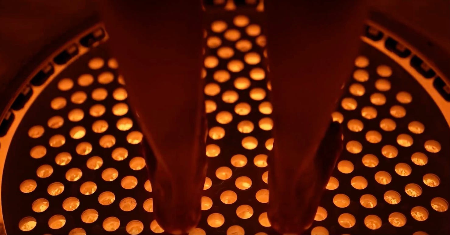
Sup Curious Clan! ✌️ This week brought one of those quiet milestones that the silicon nerds among us will remember long after the latest IPO headline fades. At the IEEE/JSAP VLSI Symposium, the powerful pioneers at imec, ASML and TSMC unveiled a world first: complementary 2D-material transistors built on a full 300mm wafer at a 50nm contacted poly pitch. For over a decade these 2D materials have been a lab curiosity that never quite survived the trip to the fab. That’s changing now. 🔬🧱
Let’s unpack why that matters. A transistor is just a tiny switch, and a modern chip has tens of billions of them flicking on and off to do everything your phone or laptop does. For 60 years the industry has made those switches faster by making them smaller, but silicon, the material at the heart of every chip, starts misbehaving when you shrink it past a certain point: electricity leaks where it shouldn’t and the switch gets unreliable.
That’s where “2D materials” come in. 🏗️
These are sheets just a single layer of atoms thick (hence 2D, since they’re essentially flat), with exotic names like ‘molybdenum disulfide’ and ‘tungsten diselenide’. Because they’re so impossibly thin, they keep tight control over the electricity flowing through them even at sizes where silicon falls apart, which makes them one of the most promising candidates to keep chips improving once plain silicon runs out of road.
So why is this week’s news a big deal and not just another lab result? Two reasons.
1️⃣ The team did it on a “300mm wafer,” the standard silicon size that real factories actually use, rather than a tiny hand-made test sample, which is the difference between a recipe that works in your kitchen and one that works in a commercial bakery.
2️⃣ They hit a “50nm contacted poly pitch.” Remember my explainer of the imec roadmap? This CPP means they packed the switches tightly enough to mimic the most advanced chips made today. They also made both flavors of switch a working chip needs, the “n-type” and “p-type” (think of them as a matched pair that work together, one handling the on, the other the off), and a remarkable 94% of them actually worked.
The how is genuinely clever too. The team used a single pass of EUV lithography to image transistor channels as small as 28nm. But they also flipped the usual recipe, building the electrical contacts first and laying the wafer-thin 2D material on top afterwards, an “innovative reverse fabrication flow” that gave near-ideal switching. As ASML’s Etienne De Poortere put it, the sharper resolution of EUV is what made channels this small possible, while imec’s Gouri Sankar Kar called the 50nm pitch a world first achieved without sacrificing performance. This is such an interesting era for materials research in chip manufacturing. A new era is being engineered into existence, one 300mm wafer at a time. 👏
Have a good week, stay safe and sound,

👨💻The round-up in sci-tech💡

🇪🇺🎙️ Europe 2031 (Europe 2031)
Highly recommend you find 2 hours to take this story in! I listened to the podcast version of this amazing manifesto on a beach in Greece and it hit home. This story looks ahead to Europe’s technological and AI future by 2031. And it’s not a pretty picture if you extrapolate the current trends.
🧠 The AI deepfake fighter (The New York Times) 🎁
A profile of digital forensics pioneer Hany Farid and his work detecting AI-generated deepfakes, which is an increasingly urgent battle as synthetic media becomes harder to distinguish from reality.
“This tool seems to have conflated sources, exaggerated claims, and injected references to agentic AI that were copied into the final report without verification.”
🤖 KPMG allegedly published an AI report filled with hallucinations (PCMag)
KPMG is under fire after allegedly publishing a report riddled with AI-generated hallucinations. It is a cautionary tale about over-relying on LLMs in professional work.
💻 SpaceX agrees to buy AI coding agent Cursor for $60 billion (The Wall Street Journal) 🎁
SpaceX has agreed to acquire Cursor, the fast-growing AI coding tool, for $60 billion. This formalizes the option deal floated earlier this year and folds one of the hottest AI developer products into Musk’s empire.
🩺 Midjourney’s full-body ultrasound scanner (Midjourney)
Midjourney, best known for AI image generation, announced “Midjourney Medical”: a full-body ultrasonic scanner that uses sound and water (no radiation or magnets) to produce a 3D body map. The company is even building spa-like facilities where you can get scanned, with the goal of a sub-60-second full-body scan. The social buzz, which includes doctors and radiologists weighing in, seems interested and skeptical.
🔬 Applied Materials unveils SenZ, a fully integrated visual system (Applied Materials)
Applied Materials introduced SenZ, a fully integrated visual inspection system for advanced chip manufacturing, aimed at improving defect detection and process control at the leading edge.
🔋 The startup using 3D printing to reinvent battery technology (The Wall Street Journal) 🎁
A startup is applying 3D printing to battery manufacturing, aiming to reinvent cell design and production. This potentially enables new form factors, higher energy density, and more flexible manufacturing.
🎬 How Toy Story 5 saved Pixar (The Wall Street Journal) 🎁
With Toy Story 5 hitting theaters on June 19, the WSJ goes inside the making of the film and how the franchise became a creative and commercial lifeline for Pixar.
🤓This week in chips⚠
🔗 ASML CEO warns of possible supply constraints on Musk’s Terafab (Bloomberg)
ASML Holding NV Chief Executive Officer Christophe Fouquet said the chip equipment maker has to make sure it doesn’t experience supply constraints when servicing new projects such as Elon Musk’s Terafab.
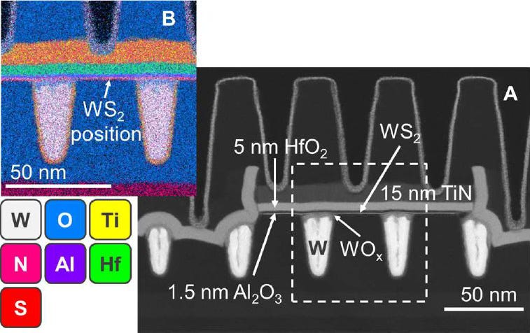
🤝 ASML, TSMC and imec bring industry-ready 2D-material transistors closer with breakthrough 300mm integration (imec)
At the 2026 IEEE/JSAP VLSI Symposium, imec, ASML and TSMC demonstrated complementary 2D-material transistors (MoS₂ and WSe₂) at a 50nm contacted poly pitch on a 300mm wafer. That’s a world first. Using a single EUV exposure to print 28nm channels, 94% of the transistors switched correctly, marking a key step toward post-silicon logic.
🔬 LPDDR6: Samsung & SK Hynix at ISSCC 2026 (More Than Moore)
Dr. Ian Cutress digs into the LPDDR6 memory presentations from Samsung and SK Hynix at ISSCC 2026. What does the next generation of low-power DRAM means for mobile, AI, and beyond?
🧠 AMD acquires Mext for memory optimization (AMD)
AMD acquired Mext, a startup whose AI-driven predictive memory technology makes flash storage behave more like DRAM, expanding usable memory capacity and easing one of the biggest bottlenecks in AI data centers.
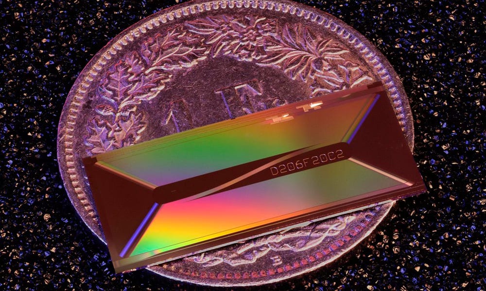
🔬 EPFL builds photonic chip that rivals much larger laboratory lasers (Optics.org)
Researchers built the first integrated ultrafast laser to rival table-top femtosecond systems, delivering 1.05 nJ pulses as short as 147 fs on a chip the size of a coin. Using an overlooked Mamyshev oscillator design, the 42cm cavity folds into a match-head-sized space and could be mass-produced at wafer scale for cheaper sensing, spectroscopy, and optical atomic clocks.
📈By the numbers📉
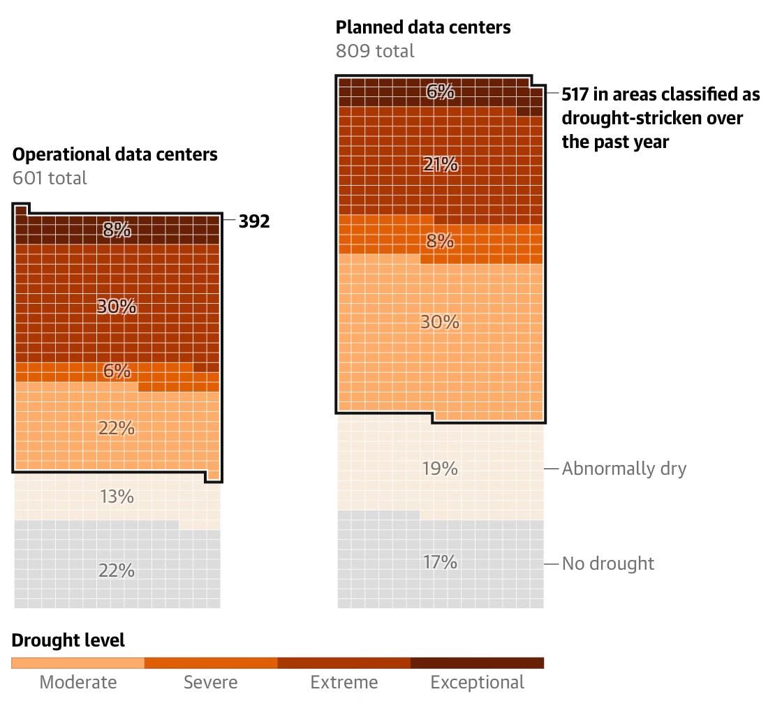
💧 AI is set to consume up to 600 billion gallons of water by 2030 (Tom’s Hardware)
New projections estimate AI could consume up to 600 billion gallons of water by 2030, with rising data-center energy consumption the primary driver. It is a stark reminder that the AI buildout’s constraints are increasingly physical: power, cooling, and water.
❤️For the love of tech❤️
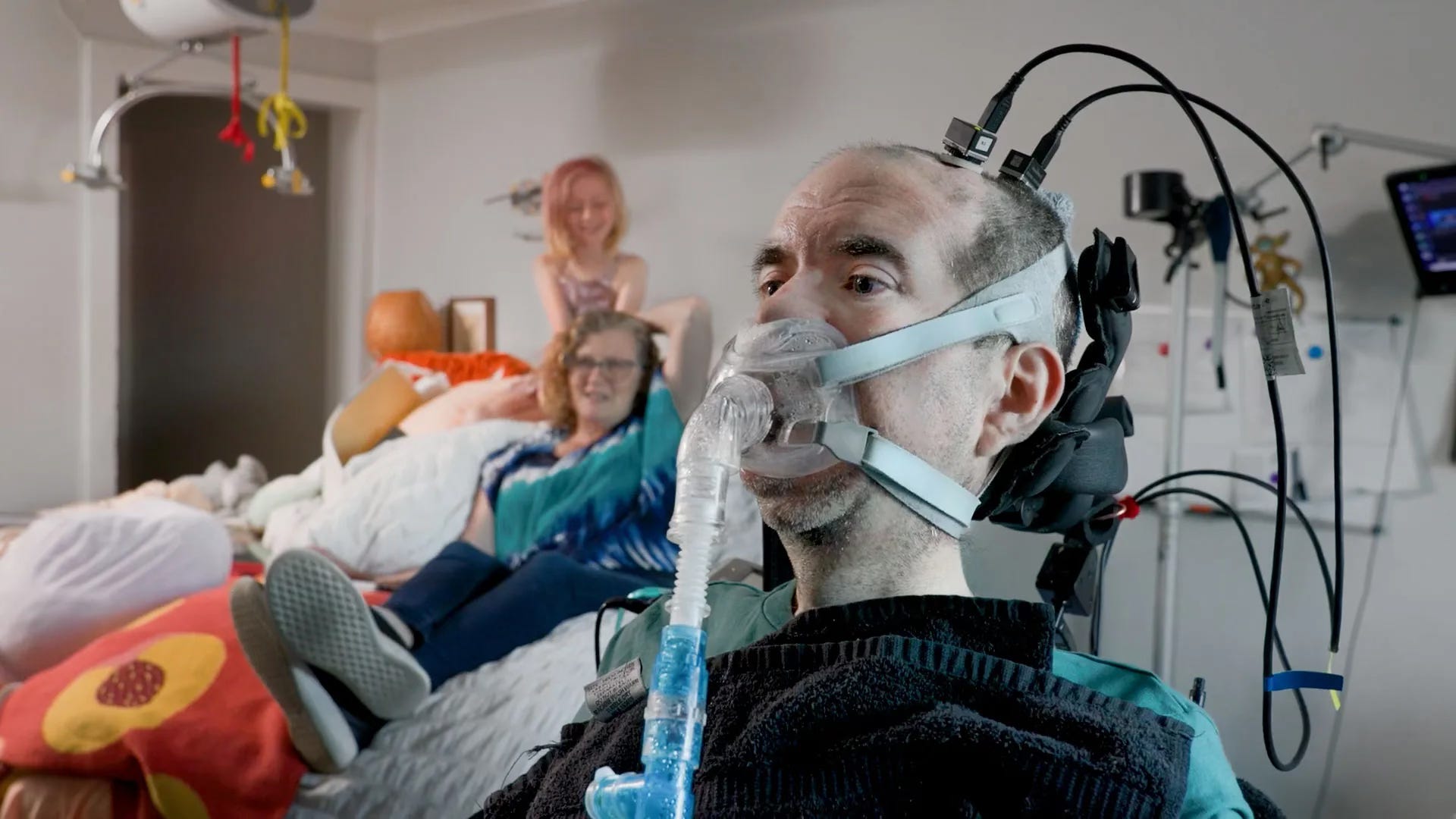
🧠 This man with ALS is “the first power user” of a brain implant that lets him speak (MIT Technology Review)🔐
Casey Harrell, paralysed by ALS, has logged more than 3,800 hours at home over 22.6 months using a brain-computer interface that lets him speak, surf the web, and do his job…largely independently! Pretty amazing. Researchers call him “the first power user of a speech BCI.” Features added along the way include a privacy mode and a profanity filter so he can read to his daughter. In his words, the device is “nothing short of revolutionary.”
Always Be Curious is the personal newsletter of Sander Hofman, Communications Manager at ASML. Opinions expressed in the introduction of this curated newsletter are my own and do not necessarily reflect those of my employer.