
Decoding imec's new industry roadmap for Logic innovation
A tour of the newest Logic roadmap for the uninitiated. Time to scale and stack our way to 2041!

It’s the week of the imec’s ITF World 2026 and newly minted CEO Patrick Vandenameele just updated the industry’s Logic roadmap. 🔥 This roadmap is a powerful navigational tool that helps the chip industry innovate from today to tomorrow. Look closely and you’ll see it’s packed with metrics, acronyms, and diagrams. So what’s actually on there? Let me walk you through all the key stuff. 👇
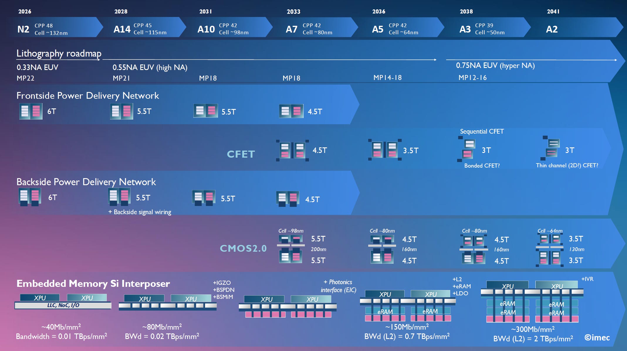
🔢 The node cadence: From N2 to A2 (2026 to 2041)
The top row shows chip “nodes”, from today’s N2 (the “2 nanometer node”) all the way to A2 (the “2 angstrom node”, with 2 angstrom = 0.2 nanometer) around 2041. And let me burst your bubble: N2 doesn’t actually mean 2 nanometers of anything physical on the chip. It’s industry marketing. The numbers stopped reflecting actual transistor dimensions years ago. There are other numbers that do mean something, but I’ll get to that in a sec. What a node name does represent is a generational marker, each step promising meaningful chip improvements in density, performance, and power efficiency. And each node will deliver waves of innovation to the world, some of which might have that next “killer product”, because that’s what makes it worth it for chipmakers in the first place.
📐 Metrics with meaning: metal pitch (MP), contacted poly pitch (CPP) and cell height
You see that each node on the new roadmap has two numbers attached: CPP and cell height. And under “Lithography roadmap”, you’ll spot another series of numbers: MP. These are metrics that actually quantify scaling. Let’s get into it.
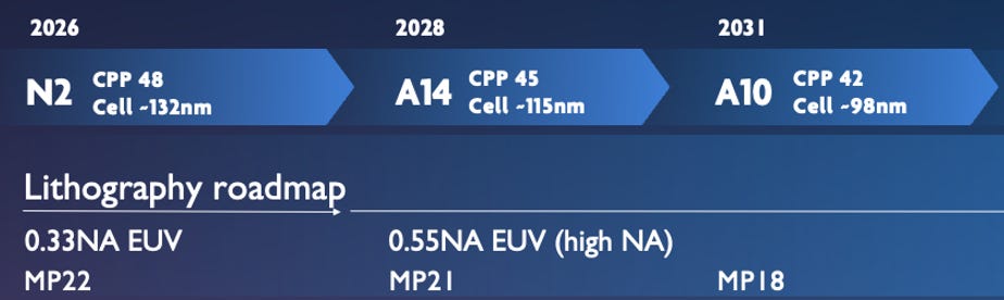
Logic designs are done by using standard logic cells (think: the building block for every gate in the chip) and CPP, or Contacted Poly Pitch, is a major driver of standard cell width. While it consists of a few elements, it comes down to the minimum center-to-center distance between transistor gates. It drops from 48nm at N2 to 39nm at A3. That’s how close transistors sit next to each other.
Cell height, then, is the vertical dimension of a standard logic cell. It shrinks from roughly 132nm at N2 to around 50nm at A3, almost a 3x reduction.
Combine the two above and you get the area of a standard cell, and from there, density.
Then Metal Pitch is the minimum center-to-center distance between neighboring metal wires, shrinking from 22nm at N2 down to 12-16nm at A3. This is another real physical density metric, and it basically tells you which lithography technology makes each node possible.
Now then, think back to what I said about those marketingy node names. Well, metrics like CPP and MP correspond to actual physical structures on the chip and are why each node delivers real density gains.
🧱 Transistor innovation: FinFET → GAAFET → CFET → 2DFET
On to the building blocks: the transistors! Quick refresher on them.
Close your eyes for a sec and imagine a chip as a metropolis. 🏙️
It’s a busy place, with lots of buildings, skyscrapers, highways. And everywhere you look on the street, you see doors. 🚪 Billions of them. Thankfully, each door can be reached by the metropolis’ intricate road network. If you want to get anything done in this town, you’ll have to start opening doors to find what you’re looking for.
Time to dip our toes in the real tech. A chip contains billions of transistors with gates (doors!). All these transistors are interconnected (roads) and they act as switches for electrical current (that’s you, opening doors). The key elements of the transistor are the gate (which modulates conductivity through a channel), the source (where drive current enters the channel) and the drain (where the current leaves the channel). So gates basically turn the transistors on and off, either allowing or preventing current to pass through. This allows the electrical currents to access, send, receive and process digital data as instructions and information. 0️⃣1️⃣1️⃣0️⃣1️⃣0️⃣1️⃣0️⃣
To be an efficient switch, a transistor needs to do three things extremely well: allow as much current to flow through when it’s on ⚡️ (drive current), allow as little current to flow when it’s off 🛑 (prevent leakage) and to switch between on and off as quickly as possible 🔄 (performance). And it’s precisely these parameters that have shaped transistor innovation over the years.
FinFET (the workhorse of the 2010s and early 2020s): from around the 14nm node, the industry made the leap from 2D planar transistors to 3D FinFET, where the gate wraps around the channel on three sides of a silicon fin instead of only across its top. Much better control over current, less leakage, lower gate voltage needed. But fins can only go so high, and you can only pack so many side by side before electrical interference kicks in. We’re at that wall today.
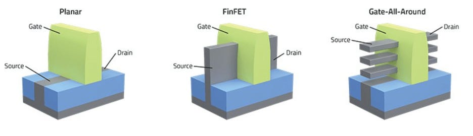
Nanosheet / gate-all-around (GAAFET): replace the vertical fin with a stack of horizontal sheets, eh voila! The gate now wraps around the channel on all four sides, further reducing leakage and increasing drive current. Chipmakers also gain flexibility to vary the width of the nanosheets to best suit a particular chip design: wide nanosheets mean higher drive current, narrow nanosheets optimize power. This is the most advanced transistor in today’s mass production and imec expects this architecture to carry the roadmap through several generations, before handing off to CFET.
Track count, the standard cell height measured in metal tracks, drops from 6T at N2 to 5.5T at A14 and A10, then 4.5T at A7. Then CFET pushes that further to 3T. Each track removed means a noticeably smaller standard cell. And that means more transistors in the same area.
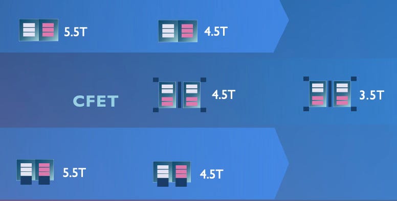
CFET (complementary FET): this is the transistor’s next leap. CFET builds on the gate-all-around concept of vertically stacked nanosheets, but makes for a taller design, stacking a pair of transistors on top of each other to essentially create two transistors in one fin. Intel has noted that their CFET experiments have shown a 30 to 50% shrink in logic circuitry. And imec foresees CFET introduction from around the A7 node (early 2030s), carrying the roadmap through A3 and into A2. The roadmap actually shows three CFET flavours: monolithic CFET (built up sequentially on one wafer), sequential/bonded CFET (n and p stacks built on separate wafers and bonded together), and ultimately thin-channel 2D-material CFET (where silicon channels are replaced by atomically thin layers). This is deep future territory.
📏 The lithography roadmap
Next up, the key manufacturing technology on the advanced Logic roadmap: ASML’s Extreme ultraviolet (EUV) lithography. It enables today's most advanced nodes and will continue to keep the pace of chip innovation.
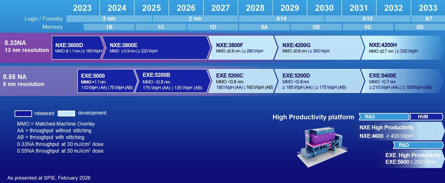
“0.33NA EUV” (the current workhorse): 13.5nm wavelength light with a numerical aperture of 0.33. This is the lithography technology that enabled the jump from 7nm through today’s most advanced nodes. ASML’s NXE systems achieve 13nm imaging resolution, with the latest NXE:3800E processing 230 wafers per hour.
“0.55NA EUV” (next gen): as chip designs continue to scale and become more complex to print economically, the door to the next generation of lithography opens. By increasing the numerical aperture to 0.55 (“High NA”), ASML’s EXE systems can image down to 8nm resolution in a single exposure. This required a complete optics redesign with bigger mirrors and an ingenious anamorphic lens design (4× reduction in one direction, 8× in the other). ASML shipped the first High NA EUV system (EXE:5000) to Intel in December 2023 for R&D, and the second-generation EXE:5200B passed acceptance testing in December 2025 at Intel’s Oregon site, marking the industry’s first commercial High NA EUV tool. The joint ASML-imec High NA EUV lab in Veldhoven has demonstrated the system’s excellent imaging performance.

“0.75NA EUV (hyper-NA)”: The first time that hyper-NA EUV popped up on an ASML roadmap was at imec’s ITF World 2024, exactly 2 years ago. A next bump in numerical aperture from 0.55 to 0.75 would further improve lithographic imaging.
⚡ Power delivery networks: from the front to the back
The next row may be the most underappreciated part of the roadmap, and one of the most consequential innovations happening in chip manufacturing right now.
Today’s chips have power delivered from the top of the chip (“Frontside Power Delivery”), which requires the power ‘lines’ to go through many layers of wiring to get to the transistors at the bottom of the stack. This means precious chip real estate has to be used for power delivery, while power is lost as it travels through those many layers. In an advanced chip, power may have to traverse 15 or more metal layers before reaching the transistors.

“Backside Power Delivery” flips the script and routes power delivery from the bottom (or ‘backside’) of the chip, gaining more direct access to the transistors via through-silicon vias (TSVs). In return, the ‘frontside’ real estate can be used to increase transistor density, while improving the overall power and performance of the chip. It also unlocks easier wafer-to-wafer bonding at the top of the die, a key enabler for 3D chip stacking.
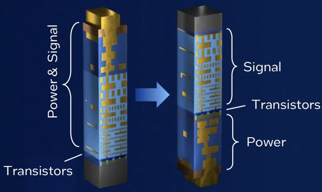
The roadmap shows two phases. First, backside power for global interconnects (the current generation, debuting in 2025/2026). Then, from A14 onward, backside signal wiring joins backside power, freeing up the frontside almost entirely for the most density-critical interconnects. The implementations by major chipmakers do differ: Intel’s “PowerVia” connects to transistor contacts, while TSMC’s “Super Power Rail” (bonus points for the awesome name, come onnn) connects directly to source and drain, which is harder to fabricate but offers greater scaling benefit. But as with any innovation: if it were easy, everybody would be doing it. This stuff requires collaborative effort across the semiconductor manufacturing ecosystem, including in deposition, etch, chemical mechanical planarisation, bonding, wafer thinning, and more.
🏗️ CMOS 2.0: the system-on-a-chip, restructured
This is a row that didn’t exist as such on earlier imec roadmaps. CMOS 2.0 is imec’s name for the post-2030 paradigm where the system-on-chip is no longer a single monolithic die, but a vertical stack of functional tiers, each built on the technology that best suits it. Dense logic on the most advanced node. Cache on a node optimized for density and cost. I/O and power management on another node. All connected together as one system. The crucial insight: not every part of a chip needs to be on the most advanced node. CMOS 2.0 reserves the most advanced (and expensive) process for the dense logic that actually benefits, and partitions everything else into tiers built with appropriate technology. The roadmap shows this with cell-height annotations like “5.5T over 5.5T” with a wafer bonding pitch in the middle.
💾 Embedded memory and the silicon interposer
The bottom row of the new roadmap shows what those systems might evolve into. That silicon interposer, man, it’s becoming an active layer in its own right.
Today’s AI accelerators sit on a passive silicon interposer (a type of electrical interface layer) that mainly carries signals between the compute die and memory stacks. The roadmap shows this evolving steadily by adding on innovations with every node. Starting at A14, the interposer gains “IGZO” transistors (indium gallium zinc oxide, a type of thin-film transistor with high electron mobility and ultra-low leakage currents), backside power delivery, and BSMiM (backside metal-insulator-metal capacitors that deliver more voltage stability, freed from that frontside real-estate constraint). At A10, the blazing speed of photonic interfaces arrives on the interposer (the “EIC”, or electronic-photonic integrated circuit), so optical I/O can finally live in-package with the compute. By A5, L2 cache, eRAM (embedded DRAM), and voltage regulators move onto the interposer. By A2, integrated voltage regulators close the loop. Crazy leaps!
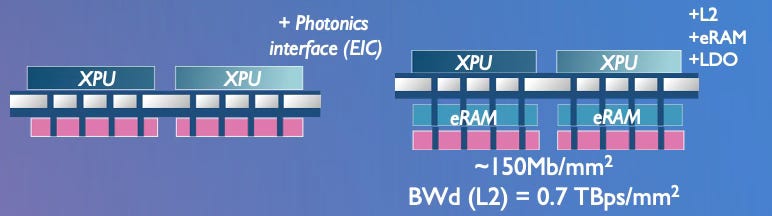
The numbers underneath tell the density story. Memory density on the interposer climbs from roughly 40 megabits per square millimeter at N2 to 300 megabits per square millimeter at A2. That’s a 7.5× increase in how much cache you can pack into the same footprint, right next to the compute die. To put it in perspective: 300 Mb/mm² means about 37 MB of memory cache in a 1 cm² interposer, before any of the actual logic die area is used.
The bandwidth jump is the even more dramatic number. The roadmap shows L2 bandwidth on the interposer going from 0.01 terabytes per second per square millimeter at A14 to 2 TBps/mm² at A2. That’s a 200× increase. Why does this matter? Because the bottleneck in modern AI accelerators isn’t compute, it’s feeding the compute with data. A GPU can do trillions of operations per second, but only if the data is there when it needs it. Every time the chip has to wait for memory, those expensive cores sit idle. Moving high-bandwidth cache from a separate memory stack onto the interposer itself, millimeters from the logic, drops both latency and energy per bit by an order of magnitude. That’s the memory wall being chipped away, one layer at a time.
💡 Zooming back out
What makes this new Logic roadmap so powerful is that it shows exactly what it takes to keep driving progress. And it literally takes an entire industry. It’s a multi-dimensional effort that touches transistor architecture, advanced lithography, power delivery, 3D integration, materials, memory cells, and packaging, all at once. The chips of 2035 will be stacks. And the silicon interposer between them will be doing real work, with photonics, cache, and voltage regulation built right in.
As the chip industry marches from the nanometer era into the angstrom era, there’s nothing stopping the engineers and scientists from dreaming up the future. But dreams aren’t enough. Thankfully, this industry’s incredible creativity and relentless focus on innovation has generated an R&D pipeline that’s filled with engineering concepts for the next 20 years. 🔥
It’s an exciting time to be part of this industry.
Sources
imec, “Orchestrating a scalable AI future”, CEO Patrick Vandenameele (May 2026)
imec, “CMOS 2.0: bringing heterogeneity inside the system-on-chip” (2024)
imec, “Outer wall forksheet: bridging nanosheet and CFET” (June 2025)
ASML, Q1 2026 financial results, presentation Investor Relations (April 2026)
imec, “Imec’s vision for 2026” (January 2026)
imec, “2D-material based devices in the logic scaling roadmap” (January 2025)
Intel, “How Collaboration in High NA EUV and Transistor R&D Are Shaping Future Waves of Device Innovation” (December 2025)
Tom’s Hardware, “Intel installs industry’s first commercial high-NA EUV lithography tool” (December 2025)
SemiEngineering, “CMOS 2.0: Layered Logic for the Post-Nanosheet Era” (August 2025)
IEEE Spectrum, “Intel Is All-In on Backside Power Delivery” (June 2023)
Excellent breakdown of imecs roadmap! I used to work there a number of years ago and appreciate the complexity of the fab process development.
A quick fact: IC fabs use Design-of-experiments to develop and optimize process recipes where they sweep a number of process parameters, measure the resulting structures, and determine the best combination of process parameters. These recipes are highly guarded IP because they took time and extensive analysis at considerable cost to determine them.