


Learn about the tiniest new transistors that will power this decade
The most advanced chips built on next-gen manufacturing processes will rely on 'gate-all-around' transistors with 'nanosheets'. And the future is about 'CFET' chips. Let's unpack the engineering.

While some continue to proclaim Moore’s Law as dead (looking at you, Jensen 👀), I find it pretty amazing to see the continued ingenuity, commitment and collaboration that goes into the extension of the chip roadmap. 💪 Moore’s Law is alive and kicking, thanks to the creativity of its stewards (TSMC, Samsung, Intel) and their grit to bring new technologies from lab to fab. The chips built on the most advanced manufacturing processes will rely on gate-all-around transistors with nanosheets. This new kid on the block will replace the older so-called FinFET transistors, which are running out of steam and cannot keep Moore's Law going. After that, as we enter the 2030s, ‘Complementary FETs’ or ‘CFETs’ are destined to take a role in chip innovation. So what the heck is a 'nanosheet'? What's gate-all-around? Why is it better? And CFET, seriously, more acronyms!? What's all the fuss about!? ⁉️ Let me take you along for a ride through some key chip designs from the past, the present and the future. I hope it helps you make sense of the headlines that you'll find in my weekly newsletter. 🤓 Disclaimer: I will by no means be complete in my story and I will definitely be cutting corners, but I'm trying to make this as accessible as possible.

So let's start with a visualization. Imagine a chip as a metropolis. It's a busy place, with lots of buildings, skyscrapers, highways. And everywhere you look on the street, you see doors. 🚪 Billions of them. Thankfully, each door can be reached by the metropolis' intricate road network. If you want to get anything done in this town, you'll have to start opening doors to find what you're looking for.
Now let's dip our toes in the real tech. So, a chip contains billions of transistors with gates(doors). All these transistors are interconnected (roads) and they act as switches for electrical current (that's you, opening doors). Gates turns the transistors on and off, either allowing or preventing current to pass through. This allows the electrical currents to access, send, receive and process digital data as instructions and information. 0️⃣1️⃣1️⃣0️⃣1️⃣0️⃣1️⃣0️⃣
To be an efficient switch, a transistor needs to do three things extremely well: allow as much current to flow when it's on ⚡️ (drive current), allow as little current to flow when it's off 🛑(prevent leakage) and to switch between on and off as quickly as possible 🔄 (performance).
Enter the transistor designs. Starting with planar.

💡 The classical transistor is called the planar transistor, because it brings together the key elements of the transistor on a two-dimensional plane: the gate(which modulates conductivity through a channel), the source(where drive current enters the channel) and the drain (where the current leaves the channel) are built on a base of the semiconducting material silicon. This transistor concept was industrialized in the 1950/60s and was highly suited for mass production and miniaturization by means of optical lithography. Transistor counts per chip quickly shot up, giving rise to Moore's Law and the chip industry as a whole. 📈
For many years, the performance of the planar transistor could be increased by shrinking the gate length. But as the gate shrank, the transistor's electrical performance started to suffer. The smaller the planar transistor, the more it leaked current. 👎 In the 2000s, at around the 20 nanometer node, this challenge drove the industry to look at alternative transistor designs.
2010s-2020s: Fin field-effect transistors (FinFET)
💡 Engineers worked out that you could exert more control over the flow of current in the channel by raising it above the plane of the silicon, like a fin in the water. The industry made the leap from 2D planar transistors to 3D FinFET (fin field-effect transistor) transistors.

In FinFET transistors, the gate wraps around the channel on three sides of a silicon fin, instead of only across its top like in planar transistors. This creates an inversion layer with a much larger surface area. That larger area gives the gate far more control over the flow of current through the transistor, while more current can flow through, there's less leakage, and a lower gate voltage is needed to operate the transistor. All good news! In addition, the vertical geometry of the FinFET allowed engineers to pack more transistors on a chip, driving Moore's Law further. The result was a chip with better performance, lower power consumption and a clear roadmap through the 2010s. 🙌😎
But Moore's Law is relentless. It was only a matter of time before FinFET technology would run out of steam. At the chip nodes that TSMC and Samsung are now rolling out, they are starting to hit the limits of how high fins can go and how many fins they can place side-by-side to boost current-carrying capacity without suffering from (you guessed it) electrical challenges.
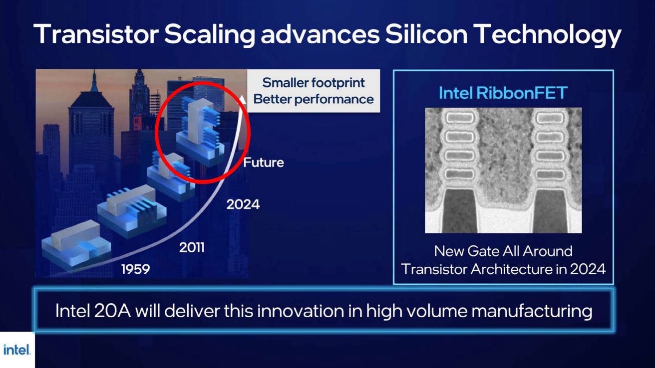
2023-2030: Gate-All-Around field-effect transistors (GAAFET)
💡 To further improve control of the transistor channel, engineers worked out that they could replace the vertical fin with a stack of horizontal sheets. This concept gave rise to the "gate-all-around" field-effect transistors: GAA transistors for short, or GAAFET if you want to be precise. According to their public statements, Samsung will start using these transistors in their new 3nm node (marketing dubbed it “MBCFET”), while TSMC is sticking with FinFETs for its 3nm but will go for GAA at 2nm.

Gate-all-around transistors use stacked nanosheets. These separate horizontal sheets are vertically stacked so that the gate surrounds the channel on all four sides, further reducing leakage and increasing drive current. That means superior electrical signals pass through and between the transistors, boosting performance of the chip. Additionally, chipmakers gain flexibility to vary the width of the nanosheets in order to best suit a particular chip design. Wide nanosheets mean higher and better drive current, while narrow nanosheets can optimize power consumption. 👍
Samsung recently started using these transistors in their new 3nm node (marketing dubbed it “MBCFET”), while TSMC and Intel have said that they are going for GAA from their 2nm nodes.
Into the 2030s: Complementary field-effect transistors (CFET)
As the chip industry marches from the nanometer era into the Angstrom era, the next transistor design in line is the complementary field-effect transistors or CFET. All of the stewards of Moore’s Law showed the recent progress they’ve made in R&D at IEEE International Electron Devices Meeting 2023, and all of them were quite bullish on the potential of this transistor.
The CFET builds on the gate-all-around concept of vertically stacked nanosheets, but makes for a taller design, stacking a pair of transistors on top of each other to essentially create two transistors in one fin. In one of its recent R&D updates, Intel noted that their experiments with CFETs have shown a 30 to 50% shrink in logic circuitry. Still, using these transistors in commercial manufacturing is still years away: industry experts estimate that CFETs could be ready for manufacturing in the next 7 to 10 years.

To unlock this step from lab to fab, a lot of innovation still needs to come from the industry as a whole. Just to name a few key areas, CFETs will need the full innovation might of the world’s higher resolution lithography systems (ASML’s High NA EUV lithography, of which the first system was just shipped to Intel), it will need a next step in etching systems that can help create that tall CFET structure, and it will require an optimized mix of materials that can deliver the appropriate electronic properties to the transistor.
As the chip industry marches from the nanometer era into the Angstrom era, there's nothing stopping the engineers and scientists from dreaming up the future. In fact, this industry's relentless focus on innovation has generated an R&D pipeline that's filled with transistor concepts for the next 20 years. 🔥
It's an exciting time to be part of this industry.
I just read this one, what an amazing and comprehensive timeline.
It was so good it reminded me of Asianometry!
Sanders, I added you. I am really sorry for the confusion and reaction. I thought Anand wrote that section, he says he linked but didn't carry over. So those were taken accross