


Stacked, standardized and supercharged: innovation trends in memory chips
The chip industry is entering a new era of memory innovation with breakthroughs spanning both DRAM and NAND chips. Let's unpack the trends.

Driven by the relentless demands of AI, high-performance computing, and next-gen mobile devices, chipmakers are reimagining memory architectures, exploring new scaling techniques, and even revisiting legacy technologies to meet tomorrow’s performance and efficiency requirements. In this landscape of rapid evolution, DRAM and NAND innovations are taking center stage, so let’s dive into what’s shaping their future.
If you get value out of my writing, then please do share this explainer with your own network and on social media. Or better yet, support ABC with a paid subscription! Thank you. 🙏
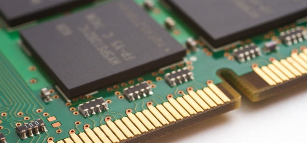
Before we dive into the latest and greatest, let’s first remind ourselves of some basics. In the memory industry, there are two types of chips that reign supreme: DRAM chips and NAND Flash chips.
DRAM (Dynamic Random Access Memory) is a volatile memory chip, meaning it only holds data as long as it’s powered. Once the power is cut, everything stored in DRAM disappears instantly. It’s the short-term working memory of a computer and its main strength is speed. It can read and write data in nanoseconds, making it the go-to choice for system memory in computers, servers, and AI accelerators. DRAM acts as a high-speed workspace, feeding processors with the data they need right now.
NAND Flash memory, on the other hand, is non-volatile, retaining data even when the power is off. That makes it ideal for solid-state drives, memory cards, and other storage devices where keeping information over time is essential. While it’s slower to access than DRAM, NAND excels in density and cost-efficiency, allowing huge amounts of data to be stored in a small space.
Together, DRAM and NAND form a complementary pair in modern computing. One is optimized for speed, the other for storage.
Now then! Let’s dive into the juicy innovations!
In DRAM, the roadmap is going 3D.
Memory makers are hitting the wall on how much smaller they can make DRAM memory cells using current 2D approaches, driving them to build upward instead of just shrinking components. Meaning, the DRAM roadmaps are increasingly powered by 3D architectures with vertical cells, followed by stacked layers of horizontal cell transistors and capacitors. The engineering challenges are immense, requiring completely new materials and manufacturing techniques.
DRAM stores information in units known as memory cells, with the area of each cell typically represented as “F².” The standard architecture to date has been the 6F² cell, featuring three vertical bit lines and two horizontal word lines. The future 4F² design reduces both to two lines, while positioning the transistor vertically to increase density and shrink chip size.
Interestingly, the major memory companies are taking different approaches. While American chipmaker Micron is planning to go directly to full 3D DRAM in a few years, Samsung and SK Hynix are currently building stepping-stone architectures, using Vertical Channel Transistor (VCT) technology.
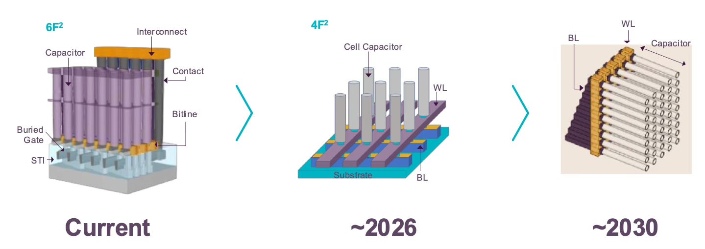
VCT can be implemented as either a FinFET design, where the conducting channel is wrapped by a thin silicon 'fin,' or as a gate-all-around transistor, where the gate material completely surrounds the conducting channel from all sides. The key innovation is that the direction of the channel in the transistor structure changes from traditional horizontal to vertical, with a gate wrapping around the channel as a switch, significantly reducing the area occupied by the device while improving storage density and performance. This vertical approach enables the industry to achieve the highly efficient 4F² cell design, which is a more compact layout that can fit 30% more memory cells in the same space compared to current 6F² designs, though it requires much higher precision in manufacturing and new materials to work reliably.
Samsung's longer-term vision for DRAM involves stacking 16 layers of memory cells, essentially building tiny skyscrapers of data storage by connecting separate wafers together—but more on that later!
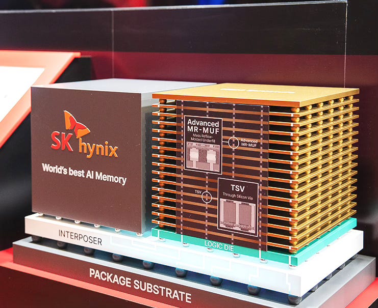
Then there’s High Bandwidth Memory (HBM), which continues to evolve at a rapid pace—and has helped crown a new memory king.
High Bandwidth Memory isn’t a new type of memory cell. Instead, it’s an industry standard on how to harness multiple DRAM memory chips to work together with logic chips. HBM vertically stacks multiple layers of memory chips on top of each other and then connects them with each other, before connecting them to the logic chip. Sounds pretty straight-forward. It’s not. 😬 A ton of innovation had to happen to make this work. To name a few key innovations:
TSVs (Through-Silicon Vias): Tiny vertical channels that allow data to move quickly between stacked memory layers.
Microbumps: Special connections between memory and processors to improve speed and reduce power loss.
Silicon interposer: A special layer inside advanced chips that basically acts like a sort of internal printed circuit board or ‘motherboard’, connecting various chips to work together.
HBM's higher bandwidth, lower power per bit transferred, and larger capacity stacks will be vital for training and running the next generation of AI models, which are projected to require memory bandwidths exceeding terabytes per second.
The AI boom has completely changed the memory space, with the High Bandwidth Memory market poised to expand at an average of 42% a year over the coming decade to over $130 billion by 2033. 📈 HBM3E production is now well underway, with Micron, Samsung, and SK hynix all charting roadmaps toward HBM4 and beyond. 🔥 Currently, newly minted memory king SK hynix leads the market with an above 50% market share, followed by Samsung with around 40%, while Micron comes in third with around 10%. There’s plenty of rivalry, opportunity and ground to be gained.
Building on HBM architectures, several memory makers are now also collaborating on High Bandwidth Flash (HBF).
It’s basically good ol’ NAND Flash, but then built in an HBM-style physical architecture like described above. SK Hynix and Sandisk are leading the charge here, having just announced a memorandum of understanding to work on standardization:
“By collaborating with SK hynix to define the High Bandwidth Flash specification, we are addressing the critical need for scalable memory in the AI industry,” said Alper Ilkbahar, Executive Vice President and Chief Technology Officer, and HBF Technical Advisory Board member at Sandisk. “This collaboration accelerates innovation and will offer the industry new tools to handle the exponential data demands of tomorrow’s applications. Our work will help provide an effective solution to meet the world’s technology needs and exceeds expectations of our respective customers.”
In short, this new memory architecture is designed to give processors (especially GPUs and AI accelerators) direct access to large amounts of NAND flash memory at very high bandwidths. It is much faster than traditional SSDs and much cheaper per gigabyte than HBM.
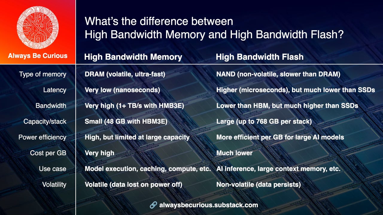
For clarity’s sake, check out the following side-by-side comparison of HBM and HBF:
In other NAND Flash news, chipmakers continue to push the boundaries of vertical scaling. 🏗️
The evolution to 3D has also been going on for a while already. NAND memory has a super dense structure, so when real estate became scarce, chipmakers started to build up to further increase bit density. Enter “3D NAND". The industry is now mass producing 3D NAND with high 200-something layers, with a roadmap to more than 1,000 (!) layers by the end of this decade.
But as layer count goes up, engineers face entirely new physical limitations. The next innovations will focus on maintaining signal integrity and reliability, allowing denser, faster, and more power-efficient storage, critical for both consumer devices and hyperscale datacenters.
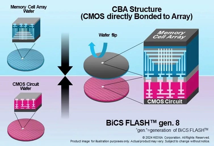
A key enabler for such innovations is wafer bonding.
In wafer bonding, the chip manufacturing process is split over multiple wafers that have to come together as one.
Originally, 3D NAND combined the logic circuitry and the layers of memory cells on a single wafer. To scale further, chipmakers are now splitting the manufacturing process: the logic circuits are made on one wafer, and the memory stack on another.
The surfaces are covered in oxide insulation and pads that link up the chips’ interconnect layers.
The bonding process then brings the logic wafer and the flipped-over memory wafer together as one, after which the memory wafer is ground down to the memory array and gets an additional interconnect layer.
And yet, innovation doesn’t always mean starting from scratch.
A nice example comes from Samsung. The Korean memory masters have revived their Z-NAND technology (first introduced seven years ago!), claiming up to 15× speed gains over conventional NAND.
While Z-NAND initially struggled to find a mass market, the AI boom has created fresh demand for ultra-low-latency storage that bridges the gap between DRAM and flash. By targeting AI inference and other performance-critical workloads, Samsung is positioning Z-NAND as a premium solution for enterprise and cloud customers.
So what’s emerging here? 🔎
It’s a memory landscape that is more diversified than we have ever seen. 🔥
Chipmakers are developing specialized memory types tuned for specific workloads: HBM for AI training, HBF for high-throughput storage, Z-NAND for ultra-low latency, and advanced 3D NAND for cost-efficient, high-density applications. This segmentation reflects a broader industry shift toward workload-optimized semiconductors, which is awesome for efficiency.
But note that chipmakers are not driving these innovations in isolation. The memory ecosystem spans controllers, packaging technologies, and interconnect standards.
And everything must evolve in parallel to enable all this innovation.
Advanced packaging techniques such as bonding technologies and through-silicon vias (TSVs) are becoming essential to stack memory closer to processors, reducing latency and energy consumption. In many cases, memory innovation is as much about integration as it is about the memory cells themselves.
So in conclusion, there’s an enormous amount of innovation happening.
The stakes are high and AI’s growth curve is outpacing Moore’s Law. Memory bandwidth and latency are fast becoming the limiting factors in system performance.
By advancing new standards like HBF, pushing 3D NAND to new heights, scaling HBM into the next generation, and reimagining legacy technologies like Z-NAND, the industry is working to ensure that memory keeps up with the compute engines it feeds.
And in the years ahead, these innovations will redefine the speed limits of the digital world. Stay tuned. 🏎️💨🔥